After the successful completion of Nano-2021 webinar, Endeavor Research Private Ltd successfully hosted the 3rd Edition of Webinar on Nanotechnology during August 02-03, 2021. The webinar was successful in gathering 38 eminent speakers from various reputed organizations and their paramount talks enlightened the gathering.
The pragmatic meet organized by Endeavor Research Private Ltd received generous response from Industrialists, Academia, Talented Researchers and Young Student Community.
The scientific program paves a way to gather visionaries through the research talks and presentations and put forward many thought provoking strategies.
Scientific sessions covered in the webinar i.e. Nanomedicine | Nanomedicine and Nano Drug Delivery Systems | Nanotechnology in Medical Diagnosis | Nanomaterials | Nanomaterials for Energy and Environmental Applications | Graphene and Applications of 2D Materials | Nanomaterials Characterizations and Devices | Nanomaterials and Nanocomposites | Nanodevices, Nanoelectronics and Nanosensors | Nano Materials Synthesis, 2D & 3D Characterization and Applications | Biomaterials and Nanobiotechnology | Nanofabrication, Nanoprocessing & Nanomanufacturing | Nano-optics
The webinar was marked with the presence of renowned Speakers, Young Researchers, Students and Business Delegates driving the two-day event into the path of success with thought provoking keynote and oral presentations.
The webinar was initiated with the honourable presence of the Keynote forum and then Oral presentations. The list includes
Speaker
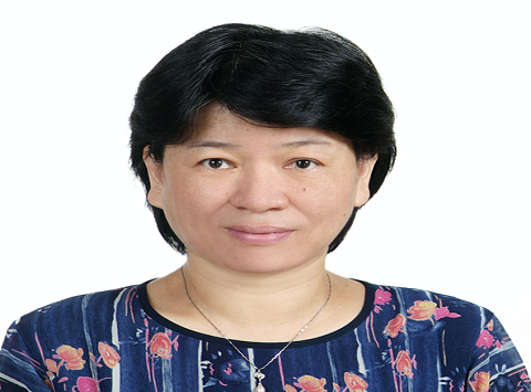
Li-Chyong Chen
Director, Center for Condensed Matter Sciences, National Taiwan University, Taipei, Taiwan
Dr. Li-Chyong Chen received her B.S. in Physics from National Taiwan University (NTU) in 1981, and Ph.D. in Applied Physics from Harvard University in 1989. Afterwards, she worked at the Materials Research Center in General Electric Corporate R&D, USA, before she joined the Center for Condensed Matter Sciences (CCMS) at NTU. Li-Chyong was the Director of CCMS and is now the Director of the Center of Atomic Initiative for New Materials. Her group is specialized in the growth of low-dimensional nanomaterials and their applications for energy, optoelectronics, and sensing. Till date she has 16 patents, 16 review articles and over 422 papers, with >17,484 citations and an H-index of 66. Li-Chyong is a Fellow of the Materials Research Society in USA, and a Laureate of the 22nd Khwarizmi International Award. She received twice Outstanding Research Award by Ministry of Science and Technology, and Academic Award by Ministry of Education.
Photo-catalytic CO2 conversion to hydrocarbon fuels, which makes solar energy harvesting and CO2 reduction reaction (CO2RR) simultaneously, is a killing two birds with one stone approach to solving the energy and environmental problems. However, challenges are the low photon-tofuel conversion efficiency of the photo-catalysts and lack of the product selectivity. Here, four cases in low-dimensional nano-materials for CO2RR will be illustrated: (i) the carbon-doped SnS2 nanosheets [Nature Comm. 9, 169 (2018)] and carbon-implanted SnS2 thin films [Nano Energy 72, 104717 (2020)]; (ii) hydrogenated Ni nanocluster-modified black TiO2 w/wo KSCNmodification [Small 14, 1702928 (2018), ACS Appl. Mater. & Inter. 11, 25186 (2019)]; (iii) MoS2 few layers with defects controlled by plasma; and (iv) direct Z-scheme ZnS/ZnIn2S4 heterostructures, comprising cubic ZnS nanocrystals on hexagonal ZnIn2S4 (ZIS) nanosheets. Vibrational spectroscopies, including Raman and Fourier transform infrared spectroscopy (FTIR), along with various electronic spectroscopies such as X-ray absorption spectroscopy (XAS) and X-ray photoelectron spectroscopy (XPS), are employed to probe the light-matterambient interactions. For instance, in-situ dark current and Raman spectroscopy measurements are used to monitor the catalyst surface affinity toward the CO2 molecule. Whereas, diffusereflectance FTIR is used to explore the CO2 and related intermediate species adsorbed on the catalyst during photo-catalytic CO2RR. Moreover, XAS and XPS can be used to monitor the electronic charge transfer behaviors. The role and interplay of the defects, surface modifications to the hosting materials, and their effects on the adsorption of CO2 and subsequent CO2RR, as well as the adsorbate-catalyst surface interactions during CO2RR will be discussed.
Speaker

Eui Hyeok Yang
Professor, Stevens Institute of Technology, USA
Dr. EH Yang is a Professor of the Mechanical Engineering Department at Stevens Institute of Technology. The first to receive a MEMS Ph.D. in South Korea, he joined Stevens in 2006 following tenure as a senior member of the engineering staff at NASA Jet Propulsion Laboratory, where he was awarded, among other honors, the Lew Allen Award for Excellence in 2003. Through the Stevens Micro Device Laboratory, he facilitated student research and hands-on education in emerging nanotechnologies and spearheaded Stevens' first undergraduate nanotechnology research training program. Dr. Yang has secured more than 35 federal grants and contracts totaling approximately $8.5 million, including funding from the National Science Foundation, Air Force Office of Scientific Research, National Reconnaissance Office, US Army, and NASA. Dr. Yang's professional service credits include editorial board positions for several journals, including Scientific Reports and IEEE Sensors Journal. Dr. Yang was a featured Track Plenary Speaker at ASME International Mechanical Engineering Congress and Exposition (IMECE) in 2018. He received the Award for Research Excellence at Stevens in 2019 and the IEEE Technical Achievement Award (Advanced Career) from the IEEE Sensors Council in 2020. Dr. Yang is a Fellow of the National Academy of Inventors. He is also a Fellow of the American Society of Mechanical Engineers.I will present the chemical vapor deposition-growth, doping, and magnetism of two-dimensional (2D) transition metal dichalcogenides (TMDs). While the lack of bandgap is a serious limitation for graphene use in electronic devices, reports have shown up-and-coming prospects of using TMDs in electronics and optoelectronics because of their unique properties, which complement graphene. In particular, 2D atomic crystals exhibiting magnetic properties provide an ideal platform for exploring new physical phenomena in the 2D limit, representing a substantial shift in the ability to control and investigate nanoscale phases. Experimental studies have shown doping of dissimilar atoms into TMDs to create 2D dilute magnetic semiconductors, which are promising candidates for spintronics applications. However, the success of these previous attempts was limited, resulting in either a Curie temperature well below room temperature or lacking scalability for practical integration into devices. Our work demonstrates a 2D dilute magnetic semiconductor at room temperature via an in situ synthesis and characterization of Fe-doped TMD monolayers. We simultaneously achieve the substitutional doping of Fe and the growth of MoS2 and WS2 monolayers and show that Fe incorporates substitutionally into Mo and W lattice sites and probes ferromagnetism in Fe:MoS2 at room temperature. This new class of van der Waals ferromagnets finds critical applications, including on-chip magnetic manipulation of quantum states or spintronics.
Speaker

Kuei-Hsien Chen
Distinguished Research Fellow and Director, Inst. of Atomic and Molecular Sciences, Academia Sinica, Taiwan
Dr. Kuei-Hsien Chen obtained his BS degree from Electrical Engineering, NTU and his MS and Ph.D. degrees from Applied Science, Harvard University in 1989. He worked on CVD diamond synthesis at General Electric R&D Center till 1992 before he joined the Institute of Atomic and Molecular Sciences (IAMS), Academia Sinica in 1993. He is currently the Distinguished Research Fellow and Director of IAMS, and adjunct research fellow in the Center for Condensed Matter Sciences (CCMS) in NTU. He works on the synthesis and applications of advanced materials, particularly on their energy applications including electrocatalysis, photovoltaic, thermoelectricity, and solar fuels. Dr. Chen has published more than 400 papers and holds 12 patents with more than 17000 citations and an h-index of 66.
Solar photoreduction of CO2 to produce value added hydrocarbons is highly desirable to tackle environmental and energy issues. Despite the great improvement in the efficiency and cost of solar cells, the efficiency in artificial photosynthesis is much lower than the >15% of solar cells. Recent progress in 2D chalcogenides with tunable bandgap and layer numbers offers great opportunity for the investigation in this field. In this work, thin film and powder SnS2 have been synthesized for the study. Hydrothermal synthesis of carbon-containing SnS2 exhibits a highly active photocatalytic conversion of CO2 to selective hydrocarbons under visible-light irradiation. Overall, the carbon doping in the SnS2 nanostructure plays a key role and significantly enhance the visible light photocatalytic activity with a photochemical quantum efficiency above 0.7%. Meanwhile, Thin film SnS2 has been grown for the mechanism study. By carbon-ion implantation of the thin film, we observed enhanced CO2 reduction under solar illumination. Other FTIR, Raman, NMR, BET, SECM, and synchrotron based facilities including APXPS and XAS have been used to investigate this issue. 1. Shown, H.C. Hsu, Y.C. Chang, C.H. Lin, P.K. Roy, A. Ganguly, C.H. Wang, J.K. Chang, C.I. Wu, L.C. Chen, K.H. Chen, Nano Letters 14, 6097-6103 (2014). 2. Shown, S. Samireddi, Y.C. Chang, R. Putikam, P.H. Chang, A. Sabbah, F.Y. Fu, W.F. Chen, C.I. Wu, T.Y. Yu, P.W. Chung, M.C. Lin, L.C. Chen, and K.H. Chen, Nature Comm. 9, 169 (2018). 3. Y. Fu, I. Shown, C.H. Li, P. Raghunath, T.Y. Lin, T. Billo, H.L. Wu, C.I. Wu, P.W. Chung, M.C. Lin, L.C. Chen, and K.H. Chen, ACS Appl. Mater. & Interface 11, 28 (2019).
Speaker

Stephen E. Saddow
Professor, University of South Florida, USA
Dr. Stephen E. Saddow received his doctorate in electrical engineering from the University of Maryland at College Park in 1993 and is currently Professor in the Department of Electrical Engineering and Professor in the Department of Medical Engineering at the University of South Florida (USF), Tampa, FL. He also is currently Collaborating Scientist at the Italian Synchrotron Light Source (Elettra, Beamline BEAR); and a Guest Researcher at the National Cancer Institute. He was elected Fellow of the AIMBE for seminal contributions to the field of Silicon Carbide (SiC) Biomedical Technology, significantly advancing in vivo biomedical devices and systems. Dr. Saddow is a Senior Member of the IEEE and National Academy of Inventors and holds more than 15 Patents, mostly on SiC biomedical device technology.
Silicon carbide (SiC) was discovered in 1891 and first saw use as an industrial material due to its hardness and wear resistance. In the 20th century a wide and variety of applications were explored due of its unique electrical and thermal properties, and it was the first light emitting diode (LED) (blue) in 1907. During the semiconductor revolution, it found application in electronics due to its high-temperature and high-voltage breakdown properties. In 1989 the first commercial blue LED was marketed using 6H-SiC, one of the many solid-state forms of silicon carbide. Today it is one of the main power electronics material systems and has found wide-spread use in electric switching applications such as electric vehicles and energy converters. In recent years there has been increased attention on SiC as a viable material for biomedical applications. Of particular interest in this review is its potential for application as a long-term implantable device for healthcare applications. SiC forms in single-crystalline, polycrystalline and amorphous forms and, while it displays ceramic-like properties, is also a wide-band gap semiconductor whereby controlled impurity doping can be used to achieve material resistivity from the semi-insulating to semi-metallic range. Numerous nanostructures have been synthesized using SiC such as nanowires, nanoparticles and nanodots. The amorphous phase is an excellent insulator which can be conformally deposited to serve as both an insulating layer as well as a biocompatible, high-durability layer for numerous implantable devices. These material properties allow the biomedical device designer to take advantage of its excellent biological, chemical, mechanical and electrical properties and realize wearable and implantable devices that display superior biological response and reliability. In addition, its potential for integration as system on a chip and those applications where SiC is used as an active material make it a suitable substrate for micro-device fabrication. This review highlights the critical properties of SiC for application as implantable biomedical devices and reviews recent work reported on using SiC as an active or passive material in biotransducers and neural implants.
Speaker
Andrew T. S. Wee
Professor, Department of Physics, National University of Singapore, Singapore
Andrew Wee is a Class of ’62 Professor of Physics, and Vice President (University and Global Relations) at the National University of Singapore (NUS). His research interests are in surface and nanoscale science, scanning tunneling microscopy (STM) and synchrotron radiation studies of the molecule-substrate interface, graphene and related 2D materials. He was a Commonwealth Fellow as well as a Rhodes Scholar at the University of Oxford, where he received his received his DPhil (1990). He holds a Bachelor of Arts (Honours) in Physics (1994) as well as a Masters degree from the University of Cambridge. He is an Associate Editor of the journal ACS Nano, and serves or has served on several other journal editorial boards.
Atomic defects are ubiquitous in a wide range of 2D transition-metal dichalcogenides (TMDs). They could be intrinsic, formed during the initial sample growth, or created by post-processing. Many properties, including optical, electrical, and chemical properties, can be significantly modulated, and potentially invoke applicable functionalities utilized in many applications. Hence, controlling chalcogen atomic defects provides an alternative avenue for engineering a wide range of physical and chemical properties of 2D TMDs [1].
This talk focuses on defects in 2D TMD van der Waals magnets, which if they exist would be ideal atomically thin building blocks for 2D spintronics [2]. Theories have predicted intrinsic magnetism in 2D VX2, such as vanadium diselenide and vanadium ditelluride. Bonilla et al. reported strong room-temperature ferromagnetism in 1T-VSe2 monolayers on van der Waals substrates [3]. We show however, that 2D 1T-VSe2 is not intrinsically ferromagnetic, but displays evidence of spin frustration [4]. Nevertheless, a magnetic transition in 2D VSe2 is induced at the contamination-free interface between Co and VSe2 via interface hybridization [5]. Promotion of ferromagnetism in 2D VSe2 is accompanied by antiferromagnetic coupling to Co and a reduction in the spin moment of Co. Consistent results are obtained for 2D VTe2 [6]. In particular, we demonstrate that the reconstructed VSe2 monolayer with Se-deficient line defects displays room-temperature ferromagnetism under X-ray magnetic circular dichroism and magnetic force microscopy, consistent with the DFT calculations [7]. This work possibly resolves the controversy on whether monolayer VSe2 is intrinsically ferromagnetic, and highlights the importance of controlling surface defects in 2D TMDs.
References
[1] Q. Liang et al., ACS Nano (2021) 15, 2165–2181
[2] W. Zhang, P. K. J. Wong, R. Zhu, A. T. S. Wee, InfoMat (2019) 1, 1–17.
[3] M. Bonilla et al., Nat. Nano. (2018) 13, 289-293.
[4] P. K. J. Wong et al., Adv. Mat. (2019) 31, 1901185.
[5] W. Zhang et al., ACS Nano (2019) 13, 8997-9004
[6] P. K. J. Wong et al., ACS Nano (2019) 13, 11, 12894–12900
[7] R. Chua et al., Adv. Mater. (2020) 200069
Speaker
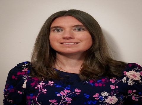
Stephanie Willerth
Full Professor, Biomedical Engineering, University of Victoria, Canada
Dr. Willerth, a Full Professor in Biomedical Engineering, holds a Canada Research Chair in Biomedical Engineering at the University of Victoria where she has dual appointments in the Department of Mechanical Engineering and the Division of Medical Sciences. She also holds an appointment with the School of Biomedical Engineering at the University of British Columbia. She serves as the Acting Director of the Centre for Biomedical Research and the Biomedical Engineering undergraduate program at the University of Victoria. She is an active member of the steering committee of the B.C. Regenerative Medicine Initiative and the Stem Cell Network. She also serves as a staff scientist at Creative Destruction Lab. She also was the President of the Canadian Biomaterials Society– serving a three-year term as President-Elect then President and Past President from 2017-2019. She recently founded the start-up company - Axolotl Biosciences.
3D bioprinting can create living human tissues on demand based on specifications contained in a digital file. Such highly customized, physiologically-relevant 3D human tissue models can screen potential drug candidates as an alternative to expensive pre-clinical animal testing. The Willerth lab has developed a novel fibrin-based bioink for bioprinting neural tissues derived from human induced pluripotent stem cells (hiPSCs), which can become any cell type found in the body. Here I will discuss the latest work from our group detailing the composition of our 3D bioprinted tissues and our new spin-off company - Axolotl Biosciences.
Speaker
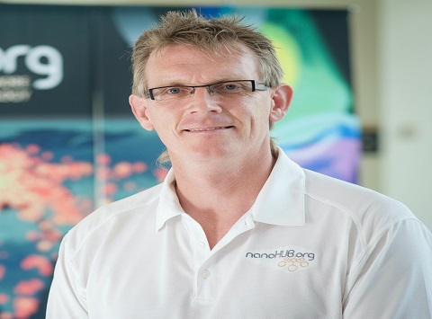
Gerhard Klimeck
Professor, Network for Computational Nanotechnology, Purdue University, USA
Gerhard Klimeck is the Reilly Director of the Center for Predictive Materials and Devices (c-PRIMED) and the Network for Computational Nanotechnology (NCN) and a Professor of Electrical and Computer Engineering at Purdue University. He guides the technical developments and strategies of nanoHUB.org which annually serves over 300,000 users worldwide with on-line simulation, tutorials, and seminars.
He was previously with NASA/JPL and Texas Instruments leading the Nanoelectronic Modeling Tool development (NEMO). His work is documented in over 500 peer-reviewed journal and proceedings articles resulting in over 20,000 citations and a citation h-index of 68 on Google Scholar. He is a fellow of the IEEE, APS, IOP, AAAS, and Alexander von Humboldt.
The downscaling of electronic devices has reached the range where the number of atoms in critical dimensions is countable, geometries are formed in three dimensions and new materials are being introduced. Under these conditions one can argue that the overall geometry constitutes a new material that cannot be found as such in nature. The interactions of electronic, photons, and lattice vibrations are now governed by these new material properties and longer-range interaction mechanisms such as strain and gate fields. The Nanoelectronic Modeling tool suite NEMO5 is aimed to comprehend the critical multi-scale, multi-physics phenomena and deliver results to engineers, scientists, and students through efficient computational approaches. NEMO5’s general software framework easily includes any kind of atomistic model and is, insofar, able to compute atomistic strain, electronics band structures, charge density, current and potential, Schrödinger eigenvalues and wave-functions, phonon spectra, and non-equilibrium Green functions (NEGF) transport for a large variety of semiconductor materials and the software is entirely parallelized. We believe that such modeling capability is not available in any other modeling tool at this time.
The NEMO modeling framework has been used to understand a variety of different device and materials concepts that will be critically important in the sub 10nm device regime. Some examples are bandstructure in Si nanowires as a function of crystal direction and strain. Interface roughness and alloy disorder scattering are modeled in the framework through an explicit atomistic representation. Gate tunneling can be modeled explicitly through quantum mechanical transport and designs can be obtained in which a good Si-based transistor is possible at 5nm gate lengths. Current developments include the explicit modeling of the metal-semiconductor interfaces, the series resistance loss and the thermal transport in nano-scale devices. Some recent examples are explorations for band-to-band tunneling transistors (BTBT) in realistic geometries in III-V, BTBT in III-N, and new 2D materials.
Speaker
Stela Canulescu
Head, Photovoltaic Materials and Systems group, Department of Photonics Engineering, Technical University of Denmark, Denmark
Dr. Stela Canulescu obtained his BSc (Physics) from the University of Bucharest and her PhD from the ETH Zurich. She is currently Head of the Photovoltaic Materials and Systems group at the Department of Photonics Engineering, technical University of Denmark. Her areas of interest are thin film kesterite solar cells and 2D materials. She has published various papers in peer-reviewed journals, such as Solar Energy Materials and Solar Cells, ACS Applied Materials and Interfaces and ACS Nano.
Pulsed laser deposition (PLD) is a powerful method for the growth of two-dimensional (2D) transition metal dichalcogenides (TMDs) into van der Waals heterostructures. However, despite significant progress, the defects in 2D TMDs grown by PLD remain largely unknown and yet to be explored. In this paper, we will combine atomic resolution images and first-principles calculations to reveal the atomic structure of defects, grains, and grain boundaries in mono- and multilayer TMDs grown by PLD. We will show that sulfur vacancies and MoS antisites are the predominant point defects in monolayer MoS2. We predict that the aforementioned point defects are thermodynamically favorable under a Mo-rich/S-poor environment. The MoS2 monolayers feature nanometer size grains connected by a high density of grain boundaries. In particular, the coalescence of nanometer grainsresults in the formation of 180° mirror twin boundaries consisting of distinct 4- and 8-membered rings. We show that PLD synthesis of bilayer MoS2 results in various structural symmetries, including AA′ and AB, but moiré patterns with various stacking angles. Moreover, we report on the experimental demonstration of an electron beam-driven transition between the AB and AA′ stacking orientations in bilayer MoS2. These results provide a detailed insight into the atomic structure of monolayer MoS2 and the role of the grain boundaries on the growth of bilayer MoS2, which has importance for future applications in optoelectronics.
Speaker
Chi Hwan Lee
Associate Professor, Purdue University, USA
Dr. Chi Hwan Lee is the Lesli A. Geddes Associate Professor of Biomedical Engineering and Associate Professor of Mechanical Engineering at Purdue University. Prior to joining Purdue in 2015, he was a postdoctoral research associate in Department of Materials Science and Engineering at University of Illinois at Urbana-Champaign. He received M.S. and Ph.D. degrees in Mechanical Engineering from Stanford University in 2009 and 2013, respectively. His scholarly efforts are dedicated to addressing unmet clinical needs using novel yet simple wearable devices with a clear path towards translation to produce measurable clinical and economic impacts. These wearable devices, which resemble sticker patches, can be easily integrated with the human body or biological cells and tissues at their length scale in a minimally invasive manner. The potential application of these devices is boundless ranging from artificial skin to drug delivery patch, and to tele-rehabilitation systems. He has published > 60 journal papers with the total citation of > 4,700 and h-index of 32. He has issued 4 U.S. patents, and > 6 utility (non-provisional) and > 20 provisional patents, leading him to spin off 3 startup companies. He has recently received the 2019 NIH Trailblazer Young Investigator Award, 2020 Purdue Faculty Award of Excellence for Early Career Research, and 2020 Purdue Focus Award.
Advanced materials engineering and processing technologies provide means to realize a range of ultrathin, flexible and stretchable bio-integrated electronics, opening up a new prospect in many biomedical devices and technologies. The mechanical flexibility and stretchability allow the devices to intimately integrate with biological systems such as biological cells, organs, and skins at their length scale. The embedded semiconducting nanomaterials provide the functionalities that can monitor the clinically useful bio-signals with sufficient spatial and temporal controls. This presentation will introduce two different kinds of novel transfer printing methods by exploiting controlled ‘cracks’ that enable the physical separation of diverse bio-electronics from their original fabrication silicon wafer, thereby can be utilized in many wearable and implantable biomedical applications. Conformal skin-mountable sensors and cell- or tissue-injectable silicon nano-needles will be discussed to show the representative applications in wearable healthcare monitoring and intracellular/intratissue drug delivery. Discussions about the results of detailed experimental and theoretical studies will be followed to reveal the essential attributes of the materials, mechanics, fabrication processes, and system configurations.
Speaker

Benoît H. Lessard
Associate Professor, Department of Chemical and Biological Engineering, University of Ottawa, Canada
Benoît H. Lessard is a Tier 2 Canada Research Chair and Associate Professor in the Department of Chemical & Biological Engineering at University of Ottawa. Recipient of 2018 Ontario Early Researcher Award, 2015 Charles Polanyi Prize in Chemistry and 2018 J. Mater. Chem. C Emerging Researcher. Since 2008, Prof. Lessard has published 97 peer reviewed journal articles, 14 patent applications, 1 book chapter and presented his work over 90 times at international and national conferences. Prof. Lessard is co-founder of Ekidna Sensing inc, which is a spinoff company based on cannabinoid sensors. Prior to joining uOttawa, Prof. Lessard was NSERC Banting Fellow at the University of Toronto on organic electronics and obtained his PhD (2012) from McGill University in Polymer reaction engineering.
Ultrapure semiconducting single-walled carbon nanotube (sc-SWNT) dispersions produced through conjugated polymer sorting are ideal candidates for the fabrication of solution-processed organic electronic devices on a commercial scale. Protocols for sorting and dispersing ultrapure sc-SWNTs with conjugated polymers for thin-film transistor (TFT) applications have been well refined. Conventional wisdom dictates that removal of excess unbound polymer through filtration or centrifugation is necessary to produce high-performance TFTs. However, this is time-consuming, wasteful, and resource-intensive. We challenge this paradigm and demonstrate that excess unbound polymer during semiconductor film fabrication is not necessarily detrimental to device performance. The following presentation will focus on the engineering of sc-SWNTs based electronic devices. The choice of conjugated wrapping polymer and its effect on film formation and the device performance leading to several emerging structure property relationships and a roadmap to high performance.
Speaker

Jean Duhamel
Full Professor, Institute for Polymer Research, Waterloo Institute for Nanotechnology, Canada
Jean Duhamel obtained his PhD in Chemical Engineering in 1989 at the Institut National Polytechnique de Lorraine (France) with Dr. André where he learned about the fundamentals of fluorescence. From 1990 to 1993, he was a post-doctoral fellow with Prof. Winnik at the University of Toronto (Canada) where he applied fluorescence to study polymers in solution. In 1993, he moved to the University of Pennsylvania (USA) as a post-doctoral fellow to study oligonucleotides by fluorescence anisotropy with Prof. Ponzy Lu. In 1996, he joined the University of Waterloo, where he is now full professor. At Waterloo, his research focused on applying pyrene excimer fluorescence to characterize the internal dynamics and structure of macromolecules in solution. His key contribution was the development of new mathematical models that enabled the interpretation of these experiments to obtain truly novel information about a variety of different polymer systems.
The abundance, bioavailability, and biodegradability of polysaccharides make them ideal target for use as industrial feedstocks, particularly as plastics. Unfortunately, natural polysaccharides do not have the range of properties required for industrial plastics, thus requiring their chemical modification. However, to be effective, chemical modifications need to account for the structure of the polysaccharides, which is not always well-defined, as some polysaccharides of interest like glycogen or amylopectin are extremely large macromolecules several 10’s of nm in size, whose highly branched interior and polydispersity complicate their characterization. This presentation will describe how the short range process of excimer formation between an excited and a ground-state pyrenyl label covalently attached onto a polysaccharide can be taken advantage of to yield quantitative information about the conformation of polysaccharides.
In these experiments, a pyrene dye is covalently attached onto the polysaccharide. Since pyrene excimer formation (PEF) occurs within ~ 5 nm, the rate of PEF is proportional to the local concentration [Py]loc of pyrene within a subvolume ~ 5 nm in diameter inside the polysaccharide, where [Py]loc is itself related to the local density of the polysaccharide. Analysis of the fluorescence decays acquired with the pyrene-labeled polysaccharides yields the number of anhydroglucose units (AGUs) confined within ~ 5 nm, which in turn provides information about the arrangement of internal helices in the polysaccharide interior. This methodology showed that in solution, amylopectin consists of clusters of helices, where the helices are separated by ~ 3 nm with the clusters being connected to each other via long oligosaccharide chains. In glycogen, another highly branched polysaccharide, the internal helices were experimentally found to be within ~ 2 nm from each other, as theoretically predicted by the Tier model. Consequently, these PEF-based experiments provide a useful means to probe the interior of complex polysaccharides at the molecular level.
Speaker

Wenwan Zhong
Professor, Department of Chemistry, University of California, USA
Dr. Wenwan Zhong is a Professor of Chemistry at University of California, Riverside. She obtained her B.S. from University of Science and Technology of China, and Ph.D. from Iowa State University. Her research is devoted to developing innovative analytical techniques to advance our understanding on how biomolecules function and to improve disease diagnosis and treatment. Her group combines synthetic receptors, functional nucleic acids, and nanomaterials, with analytical techniques like flow cytometry, open-channel separation, optical spectroscopy, and mass spectrometry, for the discovery and analysis of biomarkers. Her group is also interested in developing analytical techniques for the study of nano-bio interface.
Engineered nanomaterials (ENMs) support the growth of new and competitive technologies in the fields of energy production and biomedical science. The rapidly increasing production and applications of ENMs calls for interdisciplinary research to assess the biological impacts from ENMs and discover the fundamental factors that contribute to such impacts. My research group actively develops analytical tools to elucidate the complex interaction among ENMs, biomolecules, and biological systems. Our focus is on the biocorona formed on ENMs present in biofluids because of molecular adsorption on ENM surface. The physicochemical properties of ENMs strongly affect the formation of the biocorona, which subsequently mediates the interaction between ENMs and the biological system, making it important to study the formation and composition of biocorona, as well as their impacts on the biological behaviors of ENMs. We developed a series of analytical techniques for measurement of the binding affinity of proteins to ENMs; exploration of the interaction between a large number of proteins and ENMs in a high-throughput manner; study of the dynamics of corona formation; and investigation of the binding sites of ENMs on various proteins as well as the ENM-induced conformational changes in proteins. Recently, we developed a machine learning method for prediction of protein corona formation in biomatrices using novel descriptors other than the physicochemical properties of the ENMs to improve the prediction accuracy. These works have revealed the importance of ENM surface property on the affinity and kinetics of protein interaction; disclosed the contribution of protein characteristics to adsorption on ENMs; and compared protein and lipid corona formation in different biological fluids, including serum, tears, and lung fluid. We believe the advanced analytical tools we have developed for detailed characterization of the biocorona on ENMs can help to gain more knowledge to decipher the corona-mediated biological responses to ENMs.
Speaker

Wai-Lun Chan
Associate Professor, Department of Physics and Astronomy, University of Kansas, USA
Dr. Chan obtained his BSc degree (Physics/Materials Science) from the Chinese University of Hong Kong and his PhD degree (Materials Science) from Brown University. After two postdoctoral trainings at the University of Illinois at Urbana-Champaign and at the University of Texas at Austin, Dr. Chan started his independent research group at the University of Kansas (KU). Currently, he is an associate professor at KU. Dr. Chan is a recipient of the National Science Foundation (NSF) CAREER award (2014), and the MRS graduate student award (2006). His current research interest is on understanding the electron and exciton dynamics in a range of materials such as organic semiconductors, 2D materials, and hybrid halide perovskites.
Monolayer transition metal dichalcogenide crystals (TMDCs) can be functionalized by organic molecules to form organic-2D hybrids, which are useful for many energy and sensing applications. For light harvesting applications, processes such as excited-state charge transfer (CT) and exciton dissociation at the organic-2D interface control the overall optical-to-electrical conversion efficiency at these hybrids. In this talk, I will summarize our recent efforts in understanding microscopic mechanisms that affect the CT and exciton dissociation dynamics at organic-TMDC interfaces. Specifically, we recently found that the difference in the potential energy landscape in both lateral and vertical directions near the interface can result in distinct behaviors for two very similar interfaces. For example, effective charge separation is observed at zinc phthalocyanine (ZnPc)/monolayer-MoS2, but triplet exciton formation is observed at ZnPc/bulk-MoS2. Moreover, it is found that the dimensionality of the electron wave function and the interfacial energy level offset can affect the CT rate at organic/TMDC interfaces by more than ~20 times.
Speaker

Kaiyang Zeng
Associate Professor, Department of Mechanical Engineering, National University of Singapore, Singapore
Dr. Kaiyang Zeng is currently Associate Professor and deputy head (Graduate programme) of Department of Mechanical Engineering, National University of Singapore (NUS). He obtained his BSc (Ceramic Materials) from Hunan University, China and his PhD (Materials Science and Engineering) from the Royal Institute of Technology (KTH), Sweden. He was previously worked at the Institute of Materials Research and Engineering (IMRE), Singapore as senior research scientist before joint NUS in 2004. He currently lectures numbers of courses at NUS, including “Fracture and Fatigue of Materials” for Graduate Students, and “Fundamental of Materials Science and Engineering” for undergraduate students. At NUS, his main research area includes development of Scanning Probe Microscopy (SPM) based techniques, multifield coupling of advanced materials, deep-date analysis for SPM images, and in-situ SPM characterization of advanced functional materials. He has published more than 200 papers in peer reviewed international journals.
Piezoresponse Force Microscopy (PFM) has been widely used to characterize nanoscale ferroelectric properties since 1990s. However, the intensive study of the conventional PFM has revealed a growing number of concerns and limitations which are largely challenging its validity and application. This study will show two new developments to significantly improve the nanoscale ferroelectric measurement,, i.e., the Heterodyne Megasonic Piezoresponse Force Microscopy (HM-PFM) and Non-Contact Heterodyne Electrostrain Force Microscopy (NC-HEsFM). HM-PFM is based on the conventional instrument architecture of PFM, but uniquely uses 106 to 108 Hz high-frequency excitation and heterodyne method to measure the piezoelectric strain at nanoscale. It is found that HM-PFM can unambiguously provide standard ferroelectric domain and hysteresis loop measurements, and an effective domain characterization with excitation frequency up to ~110 MHz has been demonstrated. Most importantly, owing to the high-frequency and heterodyne scheme, the contributions from both electrostatic force and electrochemical strain can be significantly minimized in the HM-PFM measurements. Furthermore, a special technique, named difference-frequency piezoresponse frequency spectrum (DFPFS) measurement, is developed on HM-PFM and a distinct DFPFS characteristic is observed on the materials with piezoelectricity.
NC-HEsFM utilizes a newly-designed force sensor and heterodyne detection scheme to measure the nanoscale piezoelectric strain, and for the first time, achieves non-contact, electrostatic force minimized ferroelectric characterization. NC-HEsFM can perform ideal and high-resolution ferroelectric domain mapping, standard ferroelectric hysteresis loop measurement and controllable domain manipulation, and at the same time, operate on multiple high eigenmodes. NC-HEsFM also significantly minimize electrostatic force effect. Meanwhile, the application of the new force sensor makes NC-HEsFM highly compatible for high-vacuum and low-temperature environments, thus combining the advantages of non-contact operation and electrostatic force minimization, NC-HEsFM is expected to reach the ultimate goal of atomically resolved ferroelectric characterization.
Speaker

Ananth Venkatesan
Department of Physical Sciences, Indian Institute of Science Education and Research, India
Dr. Ananth Venkatesan obtained his PhD in Physics under Prof Sergey Kravchenko at Northeastern University, Boston. His thesis work was on measuring magnetization of strongly correlated 2D electrons. Since his PhD and second Post-Doc at Univ of Nottingham he has been working on a variety of mesoscopic devices. His research group at IISER, Mohali, India works on a variety of mesoscopic devices at low temperatures. Special focus is on low temperature dissipation phenomena in metallic nanomechanical resonators and novel 2D electron devices. The present work was published in Nano Lett. 2021, 21, 7, 2975–2981
Non-linearity is ubiquitous in nanomechanical systems due to the conducive aspect ratio of devices like length to thickness or width. Newtonian damping that is linearly proportional to the velocity has been successful in describing several linear and non-linear oscillatory systems. A non-Newtonian non-linear damping term of the form F = -hx2v has been observed in several nanomechanical systems fabricated out of various materials like graphene drums, Carbon nanotubes and Diamond beams. In this work we describe non-linear damping observed in sub-micron Palladium beams when driven to regimes of Duffing non-linearity. Both the Duffing non-linearity and the non-linear damping are found to be enhanced in beams exposed to low pressures of H2. The non-linear damping shows a linear drop with increase in temperature from T~110 mK to ~1 K. Such a temperature dependence at low temperatures is reported for the first time in nanomechanical systems. A non-linear analogue of the Akhiezer mechanism seems to be the most plausible mechanism. This mechanism is plausible as phonon bounce rates across the device are slower than the resonant frequency of the beam.
Speaker

Shohreh Hemmati
Assistant Professor, School of Chemical Engineering, Oklahoma State University, USA
Dr. Shohreh Hemmati is an Assistant Professor of Chemical Engineering at Oklahoma State University (OSU). She was a Postdoc at Purdue University before joining OSU in 2018. Dr. Hemmati received her Ph.D. in Chemical Engineering in 2016 from the University of New Hampshire. She obtained an M.S. in Energy Engineering in 2009 from Sharif University of Technology (Tehran, Iran), and from 2009-2012, she worked for the Sharif Energy Research Institute as a Research Scientist. She received her B.S. in Chemical Engineering in 2006 from Arak University (Arak, Iran). Dr. Hemmati’s research interests are on green nanotechnology and nanomanufacturing. More specifically, she is working on metal nanostructures synthesis, with focuses on their green and sustainable synthesis using the millifluidic techniques to be integrated with artificial intelligence (AI) for the ultimate goal of precise control over their size and morphology. Dr. Hemmati’s research is mostly funded by the National Science Foundation (NSF).
One-dimensional (1D) metal nanostructures synthesis with precise control over size and morphology is an essential way to tune their properties for practical applications in surface plasmonic, chemical/biological sensing, antimicrobial surfaces, high-performance catalysis, and transparent conductive films (TCFs) manufacturing, to name a few. Nowadays, green noble metal nanoparticle synthesis processes utilizing natural precursors are of great interest because of their advantages as the cost effective, facile, less harmful, and sustainable technologies compared to the physical and chemical synthesis methods. However, these new techniques should be optimized not only in terms of scale-up capability, but also in aspects of product quality and performance.
Our group taking different approaches for the synthesis of 1D metal nanostructures towards their green, sustainable, and continuous synthesis to overcome challenges in their physical and chemical batch synthesis methods. This presentation will include three main parts as 1) large-scale manufacturing of functionalized silver nanowire transparent conducting films; 2) protein engineering and processing of plant viral templates for controlled palladium nanorod synthesis; and 3) millifluidic, green, and sustainable synthesis of 1D silver and palladium nanostructures using tannic acid and L-ascorbic acid, respectively. Each part will also provide a fundamental understanding behind the synthesis process using different characterization techniques such as transmission electron microscopy (TEM), scanning electron microscopy (SEM), energy-dispersive X-ray spectroscopy (EDXS), and Ultraviolet–visible spectroscopy (UV-vis) as well as the kinetic studies to propose the reaction mechanism behind theses novel synthesis processes.
Speaker

Hiromu Hamasaki
Postdoctoral Fellow, Department of Mechanical Engineering, Osaka University, Japan
Dr. Hiromu Hamasaki obtained his PhD (Engineering) from the University of Tokyo in 2019. Currently, he is a postdoctoral fellow at Osaka university, Japan. His area of interest is carbon nanotubes, heat transfer and electron microscopy.
Thermal management based on nanomaterials is a fascinating topic because of their unique and excellent thermal properties. For one, carbon nanotubes show extremely high thermal conductivity; it is an order of magnitude higher than highly thermal-conductive metals such as copper. However, assemblies of the carbon nanotubes have poorer thermal conductivity than individual ones. Generally, assemblies of nanomaterials show different thermal properties from individual nanomaterials. This is mainly due to numerous, various and nontrivial boundaries in the assemblies. Although we can comprehend average properties of the boundaries based on the measurements of macroscopic specimens, it is difficult to see what is happening at the microscopic boundaries. Here, we have conducted visualization experiments of temperature distribution in a transmission electron microscope by utilizing phase transition of metal nanoparticles. In our study, temperature distribution of bundled carbon nanotubes is investigated. The experimental results are validated by finite element analysis, and it show colossal difference of thermal conductivity between intra-nanotube and inter-nanotube transport. Our methodology can aid in visualizing nanoscale thermal transport that is not restricted to carbon nanotubes.
Speaker

Anna Pyayt
Associate Professor, Department of Chemical, Biological and Materials Engineering, University of South Florida, USA
Dr. Anna Pyayt is an Associate Professor at the University of South Florida. She is the head of the Innovative Biomedical Instruments and Systems (IBIS) lab. Dr. Pyayt joined USF after being an NSF Computer Innovation Fellow and Postdoctoral Fellow at Stanford University. She earned her dual Ph.D. in Electrical Engineering and Nanotechnology from the University of Washington. Some of her research was published in Nature Photonics and Nature Nanotechnology, highlighted in Science and Nature. She designed and developed many innovative systems and instruments including Telescopic Pixel display technology that was created in collaboration with Microsoft Research. She was also the first scientist to demonstrate a novel optical interconnect between a photonic and multiple plasmonic waveguides enabling fabrication of new Biomedical nano-chips (published in Nature Nanotechnology). Her project on Mobile ELISA point-of-care system for biomedical testing was chosen by Elsevier among thousands of papers for international news coverage.
Opto-fluidics is a field focused on manipulating fluids with light for a variety of applications. Here we present our findings on several new regimes of opto-fluidic manipulation that can be engineered using careful design of micro-currents. We theoretically optimize these regimes using COMSOL Multiphysics™ and present three sets of simulations and corresponding opto-fluidic experiments. We theoretically and experimentally demonstrate that optically controlled micro-currents can be used to capture and move around variety of microscopic objects ranging from cells and nanowires to whole live worms. We also show that optofluidic manipulation can be used for improved biomedical instrumentation and diagnostic devices.
Speaker
Jifeng Liu
Associate Professor, Thayer School of Engineering, Dartmouth College, USA
Dr. Jifeng Liu received the B.S. and M. S. degrees in materials science and engineering from Tsinghua University, Beijing, China, and the Ph.D. degree in materials science and engineering from the Massachusetts Institute of Technology. He is currently an Associate Professor and the Materials Science and Engineering Program Lead at the Thayer School of Engineering, Dartmouth College. His major research field is photonic materials and devices, including integrated photonics for ultralow energy photonic datalinks as well as nanomaterials and nanostructures for photodetectors, image sensors, modulators and solar energy harvesting. He has authored or coauthored more than 90 peer-reviewed journal papers, more than 60 conferences papers, and six book chapters, which have been cited over 11,000 times according to Google Scholar. Dr. Liu has also been granted 15 U.S. patents related to nanophotonic materials and devices. He is a recipient of NSF CAREER Award, a Fellow of the Optical Society of America (OSA), and a Senior Member of the Institute of Electrical and Electronics Engineers (IEEE).
Concentrated solar power (CSP) systems offer a great advantage over photovoltaics in overcoming the solar electricity intermittency issue because it can produce electricity using stored thermal energy at night. Generation 3 (Gen3) CSP systems require a high operation temperature ³750°C to increase the power-cycle efficiency beyond 50%, exceeding that of the best research photovoltaic cells so far (~47%). However, such a high operation temperature poses a notable challenge to high temperature materials. A critical challenge is the lack of solar selective absorbers that demonstrate both high optical-to-thermal energy conversion efficiency ηtherm approaching 95% and long-term thermal stability at >750°C in air. Existing solar absorbers either have limited ηtherm£89% or deteriorate significantly within 500h at 750°C; some of these also require costly vacuum deposition for stringent thickness control. In this paper, we present low-cost, highly scalable spray-coated transition metal oxide nanoparticle (NP) pigmented solar selective coatings on various types of Inconel alloy tube sections that are thermodynamically stable at 750-800°C in air, maintaining ηtherm>94.4% under a solar concentration ratio of C=1000 after 60 simulated day-night cycles between 750ºC and 25°C. Such a high efficiency is achieved by optimizing the d-band optical absorption spectra of transition metal ions, engineering their valences and stoichiometry for maximal absorption in the solar spectral regime and minimal thermal emittance losses in the infrared regime at the same time. We were also able to maintain or even slightly increase the efficiency when operating at 750°C in air by engineering the interdiffusion of transition metal ions between the coating and the Inconel substrate to our advantage. These results indicate that the transition metal oxide nanoparticle solar selective coatings not only provide higher efficiency, but also greatly enhanced the thermal stability for future generations of high-efficiency CSP systems.
Speaker

Naveen Kumar Reddy Bogireddy
Post Doctorate, Condensed matter physics, Institute of Physics, The National Autonomous University of México
Dr. Naveen Kumar Reddy Bogireddy obtained his Masters in Nano Technology at Vellore Institute of Technology (VIT) University, India and his PhD (Applied Sciences and Engineering) from the Autonomous State University of Morelos (UAEM), Mexico. He is previously worked in MeRITs Engineering college as assistant professor, Andhra Pradesh, India. His PhD research was based on the heterogeneous catalytic reduction of several industrial organic contaminants with major focus on developing new reusable and eco-friendly catalysts which were tested in the catalysis and sensing applications. He currently doing post doc at condensed matter physics, Institute of Physics, The National Autonomous University of México (UNAM), México. His area of interest is nanomaterials for Energy and Environmental Applications. He has published various papers in peer reviewed journals including Chemical Engineering Journal, Journal of Hazardous Materials, Catalysis Today etc.
In this work, highly stable and sustainable dual emissive heteroatom doped carbon dots (DECDs) have been synthesized under optimized conditions, characterized and applied as nano optical sensor for acetone, chromium (VI) and iron (III). The as-prepared DECDs exhibit comparable PL intensities when excited at 254 nm, covering the entire visible spectrum with a flat band signal. The stability was tested up to 48,000 s continuous excitation under Xenon flash lamp, saline solution, pH and temperature. As-prepared DECDs demonstrated an excellent fluorometric-based selectivity towards Acetone, Cr (VI) and Fe (III) which are important toxic pollutants from natural disasters like forest fires and volcanic gases, and processing of plastics, cleaning, house hold products industries and waste water. The selectivity of the nanoprobes has been tested over 28 different analytes. Further, the optical sensing of acetone was tested in commercial products and direct reduction of Cr (VI) to Cr (III) in spiked tap water samples under ambient conditions.
Speaker

Angela Wittmann
Postdoctoral Fellow, Massachusetts Institute of Technology, USA
Dr. Angela Wittmann received her BSc in Physics from the Swiss Federal Institute of Technology (ETH Zurich) and a Ph.D. in Physics from the University of Cambridge (UK) in 2019. She is currently a postdoctoral fellow at the Massachusetts Institute of Technology (USA) in the group of Prof. Geoffrey Beach at the Materials Research Laboratory. Her research explores the control of the spin degree of freedom and spin dynamics in unconventional condensed matter materials such as organic semiconductors and antiferromagnets. Using different experimental techniques, including magneto-transport measurements and x-ray imaging, she aims to tackle the challenges posed by today’s vast amount of data by developing novel ultrafast and robust spin-based memory technologies.
Organic semiconductors have recently been found to have a comparably large spin diffusion time and length [1]. This makes them ideal candidates for spintronic devices. However, spin injection and transport properties in organic semiconductors have yet to be fully understood. The efficiency of spin injection from a ferromagnetic material into an adjacent non-magnetic material is given by the spin mixing conductance geff. It can be quantified by measuring the linewidth broadening of the ferromagnetic resonance (FMR) absorption of the ferromagnet due to an increase in Gilbert damping caused by spin injection into the adjacent non-magnetic material. Here, we use this technique to systematically study spin injection from a metallic ferromagnet permalloy, Ni80Fe20, into dinaphtho[2,3-b:2′,3′-f]thieno[3,2-b]thiophene (DNTT), one of the best performing small molecule organic semiconductors to date. The unique tunability of organic materials by molecular design allows us to study the impact of interfacial properties on the spin injection efficiency systematically. We show that both, spin injection efficiency at the interface as well as the spin diffusion length in the molecule can be tuned sensitively by the interfacial molecular structure and side chain substitution of the molecule [2].
[1] S. Watanabe*, K. Ando* et al., Nature Physics, 10, 308−313 (2014)
[2] A. Wittmann et al., Physical Review Letters, 124, 027204 (2020)